Modern Architecture
With all my mumbo-jumbo about conjuring up spirits and casting spells, it’s easy to lose track of the fact that computers are real and there is a very precise and concrete connection between the programs and fragments of code you run on your computer and the various electrical devices that make up the hardware of your machine. Interacting with the computer makes the notions of computing and computation very real, but you’re still likely to feel shielded from the hardware — as indeed you are — and to be left with the impression that the connection to the hardware is all very difficult to comprehend.
For some of you, grabbing a soldering iron and a handful of logic chips and discrete components is the best path to enlightenment. I used to love tinkering with switching devices scavenged from the local telephone company, probing circuit boards to figure out what they could do and then making them do something other than what they were designed for. Nowadays, it’s easier than ever to “interface” sensors and motors to computers, but it still helps to know a little about electronics even if you’re mainly interested in the software side of things.
I think it’s a good experience for every computer scientist to learn a little about analog circuits (for example, build a simple solid-state switch using a transistor and a couple of resistors) and integrated circuits for memory, logic and timing (build a circuit to add two binary numbers out of primitive logic gates). It’s satisfying to understand how the abstract digital logic involving zeros and ones is implemented using analog circuits based on continuously varying voltage levels.
I’m not going to say much about the analog-circuit-to-digital-logic connection. However, I would like to explore the connection between digital logic and a simple model of computation upon which we can base our understanding of software. My goal is to explain how logic components support primitive operations such as adding and multiplying numbers, basic memory management such as fetching (reading) and storing (writing) data and instructions, and simple branching and sequencing as required to execute program instructions stored in memory.
9.1 Logic gates
The traditional starting point in explaining digital computers is the logic gatethat implements basic Boolean functions like AND, OR and NOT. A Boolean function(named after the mathematician George Boole(1815–1864), who is credited with the discovery of the calculus1 at the foundation of computer logic) is a function that takes 1s and 0s as inputs and provides 1s and 0s as outputs. The abstraction is that each logic gate implements a particular Boolean function whose behavior can be completely specified in a so-called truth table. In talking about Boolean functions in computers, we generally replace the traditional truth-value names true and false with the corresponding binary values 1 and 0. Here’s the truth table for a two-input AND gate:
INPUT1  INPUT2  OUTPUT
0       0       0
1       0       0
0       1       0
1       1       1
A truth table specifies the output of the logic gate for each possible combination of inputs — one row in the table for each such combination. There are two rows in the table for a gate with only one input, four rows for a gate with two inputs, and 2n rows for a gate with n inputs. As we’ll see, there are also logic gates with multiple outputs, but the number of rows depends only on the number of inputs since the output is completely determined by the input.
A two-input AND is 1 only when both of its inputs are 1. A two-input OR is 1 when either one or both of its inputs are 1; here’s the truth table for an OR gate:
INPUT1  INPUT2  OUTPUT
0       0       0
1       0       1
0       1       1
1       1       1
A three-input AND gate has an output of 1 when all three of its inputs are 1 and 0 otherwise. Here’s the truth table for a single-input NOT gate, also called an invertersince its output is the opposite of its input.
INPUT   OUTPUT
0       1
1       0
|
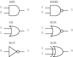
We can construct arbitrarily complex Boolean functions by connecting (“wiring together”) the inputs and outputs of logic gates. The resulting digital circuits (also called logic diagrams) are drawn using standard symbols to represent the most common logic gates. The left-hand side of Figure 8 shows the three basic logic gates whose truth tables I’ve listed. The logic gates on the right in Figure 8 can be defined in terms of those on the left.
One of the gates on the right, however, is particularly interesting. A two-input NOT AND (or NAND) gate can be constructed by feeding the output of an AND gate into the input of a NOT gate. Here’s the logic diagram for the NAND gate:
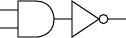 |
And here’s the truth table for the NAND gate:
INPUT1  INPUT2  OUTPUT
0       0       1
1       0       1
0       1       1
1       1       0
NAND gates are particularly versatile: you can construct any Boolean function with enough NAND gates. You can use a NAND gate to implement a NOT gate by fixing one input to be 1 and using the other input as the single input to a NOT gate, as in
INPUT1 (fixed)  INPUT2  OUTPUT
1               0       1
1               1       0
or you can simply wire together the two inputs of the NAND gate:
 |
To implement an OR gate using a bunch of NAND gates, feed each input into a NOT (implemented by a NAND) and then wire the outputs of the two NOTs to the inputs of another NAND:
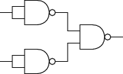 |
Another very useful logic gate shown in Figure 8 is the exclusive OR (XOR) gate defined by this truth table:
INPUT1  INPUT2  OUTPUT
0       0       0
1       0       1
0       1       1
1       1       0
And here’s how to build an XOR gate out of NAND gates:
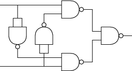 |
9.2 The digital abstraction
While logic gates and Boolean functions can be a good starting place, you may be curious about how such gates are implemented in more primitive electronic circuits. I’m wary of heading down this path: the danger is that we’ll start talking about transistors and resistors, get sidetracked by discussing Kirchoff’s current and voltage laws, descend into quantum electrodynamics, and then head off into the stratosphere waving our hands about string theory and beyond. But I think we can avoid a lengthy digression and still say a few words about how logic gates are implemented.
The most basic component in automated computing is a switch. A switch is a device that can be in one of two states, open or closed, and is such that we can change its state by physically manipulating it or sending it an appropriate signal. It’s helpful to think about the light switches in your house in considering how to use switches to implement logic gates. Put two switches in series with a light and you have an AND gate:
 |
Put two switches in parallel and you have an OR gate:
 |
Reverse the labels on a switch (“on” for “off” and “off” for “on”) and you have a NOT gate.
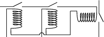
Electromechanical relays enable the output of one gate to control the inputs to other gates without someone manually closing a switch. In one of the simplest relays, an electromagnet closes a mechanical switch when the voltage drop across the coil of the electromagnet is sufficient. A small spring keeps the switch open when no current is flowing through the coil. Relays can be wired in any configuration and the switch associated with one relay can be used to control the voltage across the coil of another. Here two relays are implementing an AND gate whose output controls a third relay:
 |
Electromechanical relays work just fine as switches, and you could build a computer entirely from such relays if you had enough of them. Indeed, the first electromechanical digital computers used relays as switches.
This might convince you that it’s possible to implement logic gates, but it shouldn’t convince you it’s possible to build computers of the sort you’re probably used to working with. The problem is speed. The switches in modern computers can change from a voltage level corresponding to a binary value of 0 to a voltage level corresponding to a binary value of 1 and back many billions of times a second. Electromechanical relays can change state only a few dozen times per second. The speed of modern computers is made possible by transistors and digital integrated circuits. The transistor-transistor-logic (TTL) family of integrated circuits (ICs) defines binary values in terms of analog values: a binary value of 0 is between 0.0 and 0.8 volts and a binary value of 1 is between 2.0 and 5.0 volts.
Other families of digital ICs, based on other technologies (look up CMOS, NMOS or PMOS on the web), trade speed (how quickly the gates switch and hence how zippily your computer games run) against power (how much current is needed and hence how long my laptop operates before its batteries must be recharged) and heat (how much heat the switching circuits generate and hence how hot my laptop feels on my knees as I type these words). ICs typically package multiple gates implementing several Boolean functions (search the web for information on the venerable 7400 quad NAND, an IC that contains four NAND gates in a single package with 14 pins or places to attach wires, twelve dedicated to the eight inputs and four outputs for the four NANDs and two for power).
There are also high-density circuits with lots of tightly packed transistors called very large scale integrated (VLSI) circuits that implement the logic for an entire computer and combine millions of gates in a single package. Even so, I’ll almost guarantee that in another decade, possibly sooner, people will marvel that you and I managed with such a paltry amount of computing power. From gears and cogs to mechanical switches and electromechanical relays, from vacuum tubes to transistors and optical switches, all these technologies have been used to support the digital abstraction.
9.3 Addition and multiplication
Once you’re comfortable with logic gates, the next step is to figure out how to use them to implement primitive operations of the sort most closely associated with computers, for example, adding, subtracting, multiplying and dividing numbers. Some folks don’t think very highly of math (calculators can do it, after all) and would be much more impressed if I were to convince them that they could do something involving symbolic manipulation, say, playing tic-tac-toe, with logic gates. But we’ll stick with math for now — tic-tac-toe is trivial after computer arithmetic.
I’ll assume you know how to count and do math in different bases. We’re used to dealing with decimal or base-10 numbers, but for simplicity computers use binary or base-2 numbers since only two symbols, 0 and 1, are required in base 2, thus making logic gates particularly convenient.
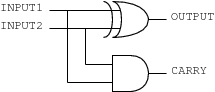
Suppose you want to add 24 and 19 in decimal. You start with the 1s column, add 4 and 9 to get 13, write down the 3 in the 1s column and carry the 1. Then you add 2 and 1 in the 10s column, add in the carry to get 4, and combine the results in the 1s and 10s columns to get the answer 43. Adding two binary numbers is no different except that columns correspond not to powers of ten (1, 10, 100, etc.) but to powers of 2: 1, 2, 4, 8, etc. Adding single-digit binary numbers (called bits) is easy because there are only four cases to consider:
INPUT1  INPUT2  OUTPUT  CARRY
0       0       0       0
1       0       1       0
0       1       1       0
1       1       0       1
You might notice that this table without the CARRY column is the same as the table for the exclusive OR gate, and without the OUTPUT column it is the same as the table for an AND gate. The function described by this table, called a half adder, can be implemented with an XOR and an AND gate:
 |
The “half” in the name is because a half adder doesn’t allow a carry bit from the next smallest column, so it works for the 1s column but not for any other. A full adder, the gate used for the rest of the columns, is described by:
INPUT1  INPUT2  CARRYIN OUTPUT  CARRYOUT
0       0       0       0       0
1       0       0       1       0
0       1       0       1       0
1       1       0       0       1
0       0       1       1       0
1       0       1       0       1
0       1       1       0       1
1       1       1       1       1
As an exercise, try to implement a full adder with two exclusive ORs, a pair of ANDs and a regular OR.
Now you should be able to string together a half adder and (m - 1) full adders to add two m-bit binary numbers. Subtraction is a little trickier and we’ll leave it the dedicated reader to figure it out or track it down on the web. (Hint: if you get stuck, search for pages on “two’s complement arithmetic.”)
One of the most basic components of a computer is a piece of digital circuitry called an arithmetic and logic unit(ALU). The ALU performs arithmetic operations like addition and subtraction and logical operations like AND and OR. (Think about what it would mean to AND together two n-bit binary numbers.) The basic ALU takes as input two n-bit binary numbers and another (generally shorter) m-bit binary number that specifies the operation the ALU is supposed to perform — addition, subtraction, logical AND, logical OR. It then provides as output the resulting n-bit number plus some additional bits that tell us such things as whether or not the result is zero and the carry output for additions in which the result is larger than n bits. The primitive operations are mapped onto binary numbers called opcodes, so, for example, 000 might be the opcode for addition, 001 for subtraction, 010 for logical AND, and so on.
Multiplication, unlike addition, is not implemented as a primitive operation performed by the ALU. There are a couple of reasons for this. First, representing the result of adding two n-bit numbers requires no more than n + 1 bits or one n-bit number and a carry bit, but representing the result of multiplying two n-bit binary numbers could require as many 2n bits to represent. And, second, as we’ll see, multiplication is considerably more complicated than addition.
Multiplication is facilitated by using circuitry for shifting the bits in a binary number; shifting to the left in binary is equivalent to multiplication. If Z = 0000XXXX is an 8-bit binary number, then Z times binary 00000010 (21 in decimal) is 000XXXX0 and Z times binary 00000100 (22 in decimal) is 00XXXX00. More concretely, 00001010 in binary is 8 + 2 = 10 in decimal; to multiply by 2, shift left one bit to obtain 00101000 in binary, which is 16 + 4 = 20 in decimal, and to multiply by 4, shift left two bits to obtain 00010100 in binary, which is 32 + 8 = 40 in decimal. Shifting to the right is integer division. Think about what happens to the least significant bits when you shift to the right.
By the way, we’re so used to how we write numbers that it’s difficult to imagine any other way. Computer engineers, however, are free to represent numbers inside the computer however they like. In most technical writing, we notate numbers by writing the digits from least to most significant starting from the right and working our way to the left. The computer jargon for this notational convention is that the digits (bits in the case of binary numbers) are represented in big-endian(“big-end-first”). This is just a convention, and there’s no reason why a computer engineer has to follow it in designing the internals of a computer. Indeed, Intel microprocessors represent numbers little-endian(“little-end-first”). The binary number 0101 is 20 + 22 = 5 big-endian and 21 + 23 = 10 little-endian. The notion of big-endian versus little-endian can apply to numbers at the bit level or to larger components of numbers such as bytes, which are components composed of eight bits. We might represent an integer in terms of two eight-bit bytes for a total of 16 bits thus allowing us to represent the integers 0 to 65535 or (using one bit as a sign bit) the numbers - 32768 to 32767.
But let’s get back to multiplying numbers. To multiply two decimal numbers, you have to remember your multiplication tables and you have to shift the intermediate results as you take into account the different columns corresponding to the different powers of ten. But once you’ve done all the shifting and applied your knowledge of the times tables, the problem reduces to addition:
   47
 * 23
 ----
  141
  94
 ----
 1081
The multiplication tables for binary numbers are pretty simple: 0 times X is 0 and 1 times X is X — that’s it! So, all we have to do is figure out how to use binary gates to shift digits and we’ve got it made:
   101 = 1 + 4 = 5 (the multiplicand)
 * 101 = 1 + 4 = 5 (the multiplier)
 -----
   101   shift 0 columns to the left and multiply by 1
    0    shift 1 column to the left and multiply by 0
 101     shift 2 columns to the left and multiply by 1
 -----
 11001 = 1 + 8 + 16 = 25 (the product)
I’ll assume that you can imagine some scheme for converting an n-bit binary number of the form 00XXXXXX into 0XXXXXX0. The entire process of multiplying two n-bit binary numbers is a little more complicated than adding two such numbers and involves a procedure, albeit a rather simple one that can be implemented in hardware.
In order to explain how to implement multiplication in hardware, we need to understand how memory is implemented. So far we’ve imagined that setting the inputs to a logic gate determines the output of the gate. In the analog circuit, we set the input wires by establishing the required voltage levels on the wires and then, after a delay for the transistors to do their thing, the right voltage values are attained on the output wires. There are times (no pun intended) when we want to save the result of a logic gate, perhaps setting it aside while we perform other computations. This is where computer memory comes into play.
9.4 Computer memory
The simplest memory units, called latchesor flip-flops, are used to store a single bit. A very simple latch called a D latch can be implemented with two NOT OR (NOR) gates:
INPUT1  INPUT2  OUTPUT
0       0       1
1       0       0
0       1       0
1       1       1
Here’s the circuit:
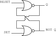 |
The output from the top NOR gate is fed back into the input of the bottom NOR gate and the output of the bottom NOR is fed into the input of the top NOR. The internal state or value of the D latch is designated as Q and the inverted value as NOT Q.
The D latch is used as follows. Normally, the inputs SET and RESET are at logic level 0. If you want to set the value of the latch to be 0, you make the RESET input go to logic level 1 for a short time. If you want to set the value of the latch to be 1, then you make the SET input go to logic level 1 for a short time.
If the SET and RESET inputs on a D latch are changing between logic levels at the same time, then all bets are off on the final value of the latch. For this reason, other memory units such as the D flip-flop use a clock signal to control when to let the memory unit change its internal state. I won’t go into clocked logic except to say that logic gates implemented with analog circuits take time to change between the voltage levels representing binary values; it is important therefore to let the voltage levels “settle out” before making use of them by, say, storing them in memory or using them in subsequent computations.
With a D latch or a flip-flop, we can store a single bit. We use registers to store larger chunks of information. A registerconsists of some number of latches, one for every bit needed. Typically we talk of registers being 16, 32, 64 or more bits wide. We use registers to store operands, the inputs to basic operations, to store the results of operations, and to store the results of intermediate calculations. In the case of multiplication, we store the operands, the multiplicand and the multiplier, in appropriately wide registers. For reasons that will soon become apparent, we make sure that the registers for the multiplicand and the product are wide enough to accommodate the product.
Here’s a simple procedure for multiplying two n-bit numbers. We’ll call the three registers the multiplicand, multiplier and product registers. The multiplicand and product registers are 2n bits wide and the multiplier register is n bits wide. The procedure modifies the contents of the multiplicand and multiplier registers as well as the product register. The additions are handled by the ALU and the shifts right and left are handled by special-purpose shifting registers. The additional logic for counting from 1 to n and implementing the conditional (if-then) statement is also handled with special-purpose circuitry. The procedure description uses a C-like or Java-like syntax, but keep in mind that the procedure is implemented in hardware.
multiply( multiplicand, multiplier ) {
    multiplicand_register = multiplicand ;
    multiplier_register = multiplier ;
    product_register = 0 ;
    for i = 1 to n {
        if the rightmost bit of the multiplier_register is 1
           then product_register =
                   product_register + multiplicand_register ;
        shift the mutiplicand_register left one bit ;
        shift the mutiplier_register right one bit ;
    }
}
Suppose the multiplicand is binary 10 (decimal 2) and the multiplier is binary 11 (decimal 3) and so n = 2. Prior to executing the for loop, the operand and result registers are initialized as:
multiplicand_register = 0010
  multiplier_register = 0011
     product_register = 0000
After the first (i = 1) iteration of the for loop, we have:
multiplicand_register = 0100
  multiplier_register = 0001
     product_register = 0010
After the second (i = 2) and final iteration of the for loop, we have:
multiplicand_register = 1000
  multiplier_register = 0000
     product_register = 0110
If we allow that primitive operations like adding two numbers or shifting a number one bit either right or left can be performed in one time step, how many time steps are necessary to multiply two n-bit numbers? Clearly multiplication is more time-consuming than addition, so it’s no surprise that engineers designing computers take considerable pains to devise circuitry for performing multiplication (and division) that runs very fast.
By the way, we needn’t restrict ourselves to operations involving only numbers. We could define primitives that operate on letters, symbols, words, sounds, images, or signals corresponding to almost anything you can imagine from brain waves to blood pressure. However, it turns out that numbers will suffice. That is, once we assemble a set of basic primitives that let us manipulate numbers, we can handle all these other forms of input by combining the numerical primitives in programs of varying complexity. There is considerable benefit in sticking with the numerical primitives, since with this minimalist approach it’s possible to build compact, inexpensive computing devices that can still perform any computation when given the appropriate software.
What’s next? Now we need to encode and execute programs that exercise these basic operations. Registers are our working memory for storing operands and intermediate results, but we need additional memory for storing programs, data and those results we’d like to keep around for a while. We need to be able to load registers with the contents of specified locations in memory, store the contents of registers in specified locations, perform operations on specified registers and store the results in other specified registers. We need to be able to perform certain operations conditionally depending on the outcome of various tests, thereby implementing conditionals and loops. And, finally, we need some way to orchestrate the whole process so that programs execute in accord with the programmer’s intuitions of how computations should proceed.
9.5 Machine language
The first part of this chapter tried to dispel some of the mystery surrounding computers by convincing you that logic gates can perform basic arithmetical and logical operations. Now I’d like to present a model of computation called the register-machine modelthat lets us string together arithmetical and logical operations to create entire programs. The register-machine model and its many variants are derived from the so-called von Neumann architecturewhose logical design is the foundation for most modern computers.
A register machine consists of a memory, a central processing unit(CPU) — also called the processor— and a pathway or bus for moving data from memory to the CPU and back. The CPU is constructed from an arithmetic and logic unit (ALU), control logic that implements the basic loop governing program execution and a bunch of registers that keep track of operands, results and other useful information.
We’ve already seen one type of memory: the registers used temporarily to store operands and results in performing basic operations like addition and multiplication. Registers of this sort play an integral role in the register-machine model, as you may have guessed from the name; however, when we speak about memory in the context of the register-machine model, we’re talking about something separate — a place to store lots of stuff for a long time.
In the register-machine model, this sort of longer-term memory is defined in terms of a set of locations in which each location has an address and contents. The addresses are generally assumed to be arranged consecutively as the natural numbers 0 through M (of course, we’ll represent addresses internally as binary numbers, but that’s merely a detail at this level of abstraction). The content of each location is an integer between 0 and N (also represented as a binary number). This model of memory is the random-access memory(RAM) model, which assumes that we can access the contents of any location in memory by simply referring to its address. If we have one megabyteof RAM (one megabyte is 210 = 1024 kilobytes, where a kilobyteis 210 bytes and a byteis eight bits) then M is 220 - 1 and N is (28 - 1) = 255. If K is the address of a location in RAM that is greater than or equal to 0 and less than or equal to (M - 1), then (K + 1) is the next consecutive address in RAM.
We’ll gloss over lots of details concerning how memory is implemented. For example, static RAM (SRAM) is implemented with the sort of latches and flip-flops we used to construct registers. Dynamic RAM (DRAM) is implemented with fewer transistors by using capacitors to store a charge determining whether a memory cell is interpreted as containing a logical 0 or 1; the charge leaks away, however, and so DRAMs must be periodically refreshed (the dynamic part), complicating their implementation and use. There are also the intricacies of using decoders and multiplexers to address a large RAM; very interesting stuff, but we’ll ignore these details. Ditto for the details of implementing the various pathways or buses used for transfers to and from memory. We’ll assume that if we have the address of a location in memory, then we can either store a number in that location or read its current contents.
Specifically, if we have the address of a location in RAM in a register of the ALU, then we can store the current contents of the RAM location in some other register in the ALU — this corresponds to reading from memory and is called “loading (the contents of) a register from memory”. In addition, if we have the address of a RAM location in a register of the ALU, then we can store the current contents of some other register in the ALU in the location in RAM pointed to by this address — this corresponds to writing to memory and is called “storing (the contents of) a register in memory”. That’s pretty much it for our model of memory. (We’re ignoring other forms of memory such as those involving magnetic and optical disks and tape drives.)
The contents of memory are interpreted differently depending on context. In some circumstances, the CPU interprets the contents of a location in memory as an instruction of one of three types: a primitive arithmetical or logical operation to be performed by the ALU, an instruction to move information between RAM and the registers of the CPU, or a conditional indicating a test and alternative actions. In other cases, the CPU might interpret the contents of a location as an address or part of an address for a location in memory. In still other cases, it might interpret the contents of a location as data to be used as operands for arithmetical or logical operations.
If the registers are large enough, then the CPU may treat their contents as segmented into two or more fields, so that, for example, the first five bits are interpreted as a code for an instruction or basic operation, the next five for an operand or an address, the next five ... well, you get the idea; there are all sorts of strategies for organizing memory. The CPU also includes a special register called the program counter(also called the instruction address register) that keeps track of where the CPU is in executing a program stored in RAM. We’ll assume (without loss of generality, as mathematicians like to say) that when the computer is first started the program counter contains the address of the first location in memory.
The basic loop governing the operation of the CPU is as follows. The CPU interprets the contents of the location in memory pointed to by the address in the program counter as an instruction and does whatever the instruction requires — for example, loading registers from memory, storing the contents of registers in memory, adding the contents of two registers and placing the result in a third register, and so on. There are also important instructions called jumpand branch instructionsthat can modify the contents of the program counter. For example, a jump instruction might specify an address (or a register containing an address) to load into the address counter. A branch instruction typically specifies a test and an address to load into the address counter if the test is positive; the test might be whether or not the number stored in a register is zero. If the contents of the program counter are not changed by a jump or a branch instruction, then the CPU increment the contents of the program counter by one so that it now points to the next location in memory. The jump and branch instructions and the default mode of incrementing the program counter govern the flow of control in programs containing loops, procedure calls, conditionals and much more.
The machine language of a particular computer is a language of binary codes that can be directly interpreted by the hardware comprising the CPU. The CPU interprets the bits stored in memory as codes for instructions, memory addresses and registers. Writing in machine language is painful because it’s very difficult for us to keep track of what all the bits mean. That said, it’s instructive to look at a simple machine-language program to get a better appreciation of what’s going on in the CPU.
|
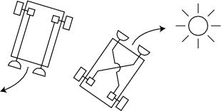
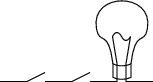
Let’s consider a program for controlling a mobile robot. Figure 9 depicts two very simple mobile robotsseen from above. Each robot has a rectangular body and two wheels, each attached to a separate motor, and two sensors that respond to light. (The robots are adapted from Valentino Braitenberg86’s book Vehicles: Experiments in Synthetic Psychology.) The sensors are photovoltaic cells: the more light that falls on the sensor, the more current it produces. The sensors are wired directly to the motors and we assume that they generate enough current to drive the motors and turn the wheels. The more the light on the sensor, the greater the current and the faster the motor turns. Depending on how the sensors are wired to the motors, the robots either turn and drive toward the light (the robot on the right) or turn and drive away from the light (the robot on the left). We’re going to implement the light-seeking robot on the right.
Instead of wiring the sensors and motors together, we’ll assume a small computer mounted on the robot can read the sensors and control the motors. The interface between the computer and the motors and sensors is similar to that used in the Lego Mindstorms Robotics Invention System. As far as the programmer is concerned, the current (double meaning here) value of each sensor is always available in a particular location in memory; external circuitry makes sure this happens. Programs read from the memory locations reserved for sensors but don’t write to them. In addition, a memory location is assigned to each motor and its content is interpreted by the external hardware as a measure of how much power to apply to the motor. So our two-motor, two-sensor robot has four locations set aside in memory: one for each sensor that a program reads from and one for each motor that a program writes to in order to control the motor.
A simple program that exhibits the desired light-seeking behavior can be implemented using bang-bang control, so called because the devices to be controlled, motors in this case, are either on or off, there’s no middle ground. The method may seem a little crude but it’s very effective. The program first checks to see which of the sensors is receiving more light. If the left sensor is receiving more, it turns on the right motor and turns off the left; if the right sensor is receiving more, it turns on the left and turns off the right. Then it loops and does the same thing over again until the batteries lose their charge or someone shuts the computer off.
In order to write this program, we need to imagine a simple computer with four registers: the program counter (instruction address register), register 1, register 2 and register 3. We’ll use decimal instead of binary numbers to make things a little simpler to understand. Assume we have 100 memory locations with addresses 00 to 99. Suppose that each register and each location in memory is large enough to store a signed ( + or - ) four-digit number. Our computer will support the set of instructions described here along with the exact way in which the instructions appear in memory, including any necessary register or address information. Obviously a real computer would have an ADDition instruction as well as SUBtraction instruction, but I’m including only the instructions I need to write this simple program. In each case, the leftmost digit of an instruction codes the type of instruction (opcode) and the remaining digits specify registers and addresses as needed.
SUBtract the contents of register i from the contents of register j and store the result in register k; a SUB instruction looks like 1ijk; for example, 1123 subtracts register 1 from register 2 and stores the result in register 3.
JUMP to location — change the program counter; an ADD instruction looks like 20mm where mm is a two-digit base-10 number indicating an address; for example, 2099 jumps to location 99.
BRANCH — if the number in register n is less than or equal to zero, then jump to location mm; a BRANCH instruction looks like 3nmm; for example, 3199 jumps to location 99 if the contents of register 1 are less than or equal to zero, otherwise the program counter is incremented as usual.
LOAD the contents of memory location mm into register n; a LOAD instruction looks like 4nmm.
STORE the contents of register n in location mm; a STORE instruction looks like 5nmm.
Now we write the machine code to drive a Braitenberg light-seeking robot.Assume that the right and left sensors write their sensor readings into locations 01 and 02 respectively, and that locations 03 and 04 are read by the right and left motors respectively, thereby determining the power available to the motors. Initially these four locations are zero. I’ve also stored the value 0000 in memory location 05 and the value 0100 in memory location 06, since it will be convenient to have these constants available to set the power to the right and left motors.
Loading a machine-language program into memory is pretty straightforward. Here’s what memory looks like with the program loaded but before the computer starts:
00    01    02    03    04    05    06    07    08    09
2007  0000  0000  0000  0000  0000  0100  4011  4022  1123
10    11    12    13    14    15    16    17    18    19
4105  4206  3316  5203  5104  2007  5204  5103  2007  0000
| |
| Figure 10: Machine code for our light-seeking robot | |
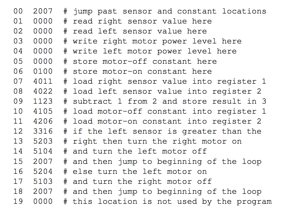
If this listing seems pretty inscrutable, then you have some idea why hardly anyone programs in machine language anymore. We can improve readability a little by listing the program one instruction to a line followed by some useful commentary. Typically, machine-code programs are listed in files along with a liberal sprinkling of commentsto help the programmer remember what all the instructions do. Figure 10 shows a listing of our machine-code program; the comments follow the sharp (#) sign. A program called a loadertakes a file containing machine code and loads it into RAM ready to run.
| |
| Figure 11: Assembly code for our light-seeking robot | |
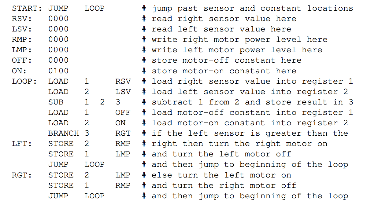
The listing in Figure 10 is still pretty difficult to understand. Part of the problem is that in a long program it’s hard to remember what all the numbers refer to; comments help but only so much. A reasonable alternative to machine code is to use assembly languagefor writing low-level programs. In assembly language, instructions are given mnemonic (easily remembered) names and we’re allowed to use symbolic addresses for memory locations. An assembler is a program that converts an assembly-language program into machine language. Among other bookkeeping tasks, the assembler figures out the machine addresses for all the symbolic addresses. Once assembled, the resulting machine code is loaded into RAM like any machine-code file. Figure 11 shows an assembly-code version of the machine code in Figure 10.
Here are some tips on understanding the code in Figure 11. After the SUB instruction, register 3 contains the contents of register 2 minus the contents of register 1, or LSV - RSV in this case. The contents of register 3 are greater than zero just in case the left sensor value is greater than the right sensor value. If the left sensor value is greater than the right sensor value, that means the light source is off to the left and we want the robot to turn left. We can drive the robot to the left by making the right motor spin faster than the left motor. If register 3 is greater than zero, then according to our specification of the BRANCH instruction, the program counter is incremented normally and the instructions at LFT and LFT + 1 are executed, setting the right motor to ON and the left motor to OFF.2 If register 3 is less than or equal to zero, then the program counter is set to RGT and the instructions at RGT and RGT + 1 are executed, setting the left motor to ON and the right motor to OFF.
The assembly-language program is still hard to read (and write) even for this relatively simple program, but its biggest drawback is that assembly language is specific to a particular machine or family of processors. The advantage of a so-called high-level programming language like C, Java or Scheme is that you can write the code implementing a procedure once and then later use various tools such as compilers and interpreters to convert the high-level specification into the machine code of as many specific computers as you like. A compileris just a program that takes as input a program written in one language and produces as output another program written in a second language (the compiler itself may be written in a third language). A programmer can use one language and one model of computation to think about procedures and processes and rely on the compiler to translate code into machine language that a particular computer can understand directly.
Here is the C-language versionof our robot control program. A good C compiler would convert this C code into machine code very much like what we’ve written but specific to the target machine of the compiler. Reviewing and augmenting our piecemeal introduction to C syntax in Chapter 4, let’s look at a few hints for deciphering the next code fragment. In C, integer variables and constants are declared with int, assignment is accomplished with =, checking whether one integer is greater than another is handled with >, conditionals look like if ( condition ) { code } or if ( condition ) { code } else { code }, while ( condition ) { code } is the syntax for a while loop, and while (1) { code } and while (true) { code } are two ways to specify a so-called infinite loop(1 and true are conditions that are always satisfied).
void seek_light() {
  int on = 100 ;
  int off = 0 ;
  while (1) {
    if (left_sensor > right_sensor) {
      right_motor = on ;
      left_motor = off ; }
    else {
      right_motor = off ;
      left_motor = on ; }
  }
}
We can specify the same computation as a recursive procedure in Scheme. Again, a good compiler will convert this specification to something that looks pretty much like the machine code described earlier. In a Scheme expression of the form (define (function arguments) (define variable value) body), the inner define introduces a local variable that is seen only in the definition of function:
(define (seek_light)
  (define on 100)
  (define off 0)
  (if (> left_sensor right_sensor)
      (and (set! right_motor on)
           (set! left_motor off))
      (and (set! right_motor off)
           (set! left_motor on)))
  (seek_light))
Compilers and interpreters let a programmer specify computations in a language that has some of the convenience and naturalness of human languages but encourages a certain discipline and level of precision that makes the job of the compiler writer easier. The programmer who writes the compiler often has to map one model of computation, for example the substitution model, onto another model, for example the register-machine model.3
You can learn about the history of computer architecture by reading about the lives of Alan Turing, John von Neumann, Presper Eckert, John Mauchly and other early computer pioneers. Most of what I know about computer hardware comes from my early training in electrical engineering and then much later from reading Computer Organization and Design by John Hennessy and David Patterson. I recommend the Hennessy and Patterson book if you want to go into any of the topics raised in this chapter in greater detail. To learn more about Lego robots, visit the Lego Mindstorms web page or check out Knudsen99’s The Unofficial Guide to Lego Mindstorms Robots. Fred Martin01’s Robotic Explorations: A Hands-On Introduction to Engineering is a more advanced introduction to building and programming small robots.
Learning about computer hardware is both interesting and useful if you program “close to the machine”. In robotics, computer networking, embedded control systems for home and automotive applications and even in designing toys containing microprocessors, it’s important to know how the hardware works and how to build interfaces to get information into and out of computers. But understanding how computer hardware works is fascinating in its own right, and as a computer programmer you’ll also find it useful in understanding all sorts of related concepts in computer science. The next chapter is a perfect example.
1 A “calculus” is any method of calculation using specialized symbolic notation, not just the invention credited to Newton and Leibniz and referred to in textbooks as differential and integral calculus.
2 We’ll assume that setting the right motor to ON makes the right wheel turn, thereby moving the right side of the robot forward, and that setting the left motor to ON makes the left wheel turn, thereby moving the left side of the robot forward. Setting a motor to OFF allows the attached wheel to turn freely. We’d have to wire the motors so as to ensure this behavior.
3 You could also write a compiler whose input is a program in one high-level language and output is a program in another high-level language, for example, compile Scheme code into Java or C code. In our introductory courses, students write a compiler that translates from Scheme to Java and then another compiler that translates from Java to Scheme. It’s a wonderful exercise for learning about programming languages and computing in general.