|
1
|
- Errors in Crossbars
- John E Savage
|
|
2
|
- General Properties of nanoarrays
- NanoFabrics – an early model for nanoarrays
- NanoPLAS – A programmable architecture
- Coping with defects
|
|
3
|
- DeHon (JETC, Vol. 1, No. 2, 2005) predicts one to two orders magnitude
greater density with nanoarrays than FPGAs realized in 22nm lithography,
even if latter components are defect-free!
|
|
4
|
- Axially doped NWs
- Resistance: 0.1MΩ (on) to 10GΩ (off) (>104
ratio)
- Radially doped NWs
- Use as shield and control spacing or to encode NW.
- Silicide – coating Si with Ni and annealing forms metallic NiSi
- Resistivity of NiSi = 10-5 Ωcm, of Si = 10-3 Ωcm
- This reduces NW contact resistance to 10KΩ
|
|
5
|
- Chen et al. [2003]:
- Ti/Pt-[2] rotaxane-Ti/Pt sandwich exhibiting state storage with
resistance change by > x10
- From 500KΩ to 9MΩ for 1600nm2 jnctn
- State switched with +/- 2V, read at +/- 0.2V
- Molecular sandwich created with Langmuir-Blodgett
- 8 x 8 crossbar constructed
|
|
6
|
- SRAM-based programmable crosspoint has area 2,500λ2
versus 25λ2 for NW crossing [DeHon 1996].
- NWs can be grown to hundreds of microns in length, but only for large
NWs.
- 10μm x 10μm arrays have been demonstrated
|
|
7
|
- NWs may break during assembly
- Diameter can be ≈100 atoms
- Statistical nature of contacts
- NW-to-MW junctions: small no. of atomic bonds
- E.g. [Huang 2001]: 95% of contacts good
- NW-to-NW junctions: composed of 10s of atoms
- E.g. [Chen 2003]: 85% of crosspoints useable
- Statistical nature of doping
- Number of dopants per NW diameter is small
|
|
8
|
- NW Defects
- Functional: Good contacts at each end, resistance within range, no
shorts to other NWs
- Defective NWs can be found through testing
- Shells on axial or radial NWs prevent shorts between NWs
- Crosspoint Defects
- Programmable (Most common state)
- Resistance can switched between design limits
- Non-programmable (More common than shorts)
- Cannot be turned on – too few molecules at junction
- Shorted into the on state (treat as defective wires)
- Cannot be programmed into the off state
|
|
9
|
- [Chen 2003] 8 × 8 crossbar within a 1 μm2 area, density
of 6.4 Gbits cm-2. Two 4 × 4 crossbar subarrays
configured to be a nanoscale demultiplexer and multiplexer that were
used to read memory bits in a third subarray. Nanoimprint litho used for
NWs
- [Wu 2005] 34 x34 crossbar memory circuits at 30-nm half-pitch
nanoimprint lithography used for NWs, LB for film deposition. Read,
write, erase and cross-talk were also investigated. Also see [Jung 2004]
|
|
10
|
- Heath and Stoddart have implemented a 400x400 array of NWs with density
of 1011 bits/centimeter.
- “Modern DRAM circuits have 140nm pitch wires and a memory cell size of
0.0408 mm2.”
- “Here we describe a 160,000-bit molecular electronic memory circuit,
fabricated at a density of 1011 bits cm-2 (pitch
33 nm; memory cell size 0.0011 mm2), that is, roughly
analogous to the dimensions of a DRAM circuit projected to be available
by 2020.”
|
|
11
|
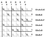
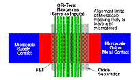
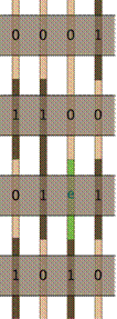
- NWs in black are drawn high by applied voltages
- Output functions shown
- Programmed crosspoints realize a routing network
|
|
12
|
- Goal: turn on one NW in each array dimension
- Earlier lectures describe
- Undifferentiated NW decoders
- Random contact decoder
- Randomized mask-based decoder
- Differentiated NW decoders
- Axially encoded NWs
- Radially encoded NWs
|
|
13
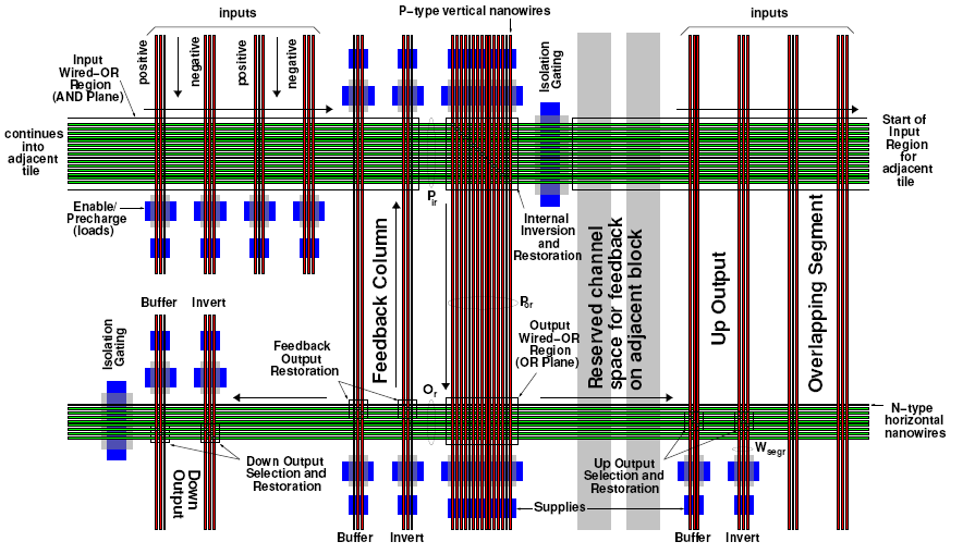
|
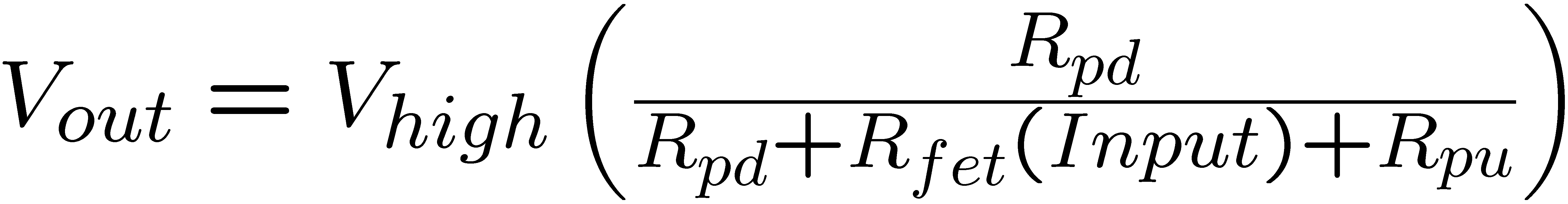
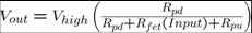
- Wire-OR non-restoring
- Capacitive coupling of input NW to vertical NW
- FET at intersection
- Gives voltage divider
- Inverter shown at right
- Reverse Vhigh and Gnd to obtain buffer
|
|
14
|
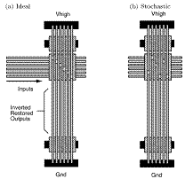
- Ideal restoration array has one FET/NW
- Stochastic assembly raises its ugly head
- Some NWs may form FETs with multiple vertical NWs
- How many vertical NWs are needed?
- A coupon collector problem
|
|
15
|
- Write
- Apply voltage across junction
- Read
- Disconnect one end of each NW
- Drive current from a NW in one dimension to NW in other
|
|
16
|
- Crossbars can be used for storage, computation or routing
- Amenable to sparing and remapping
- Challenge:
- Defect tolerance and avoidance
|
|
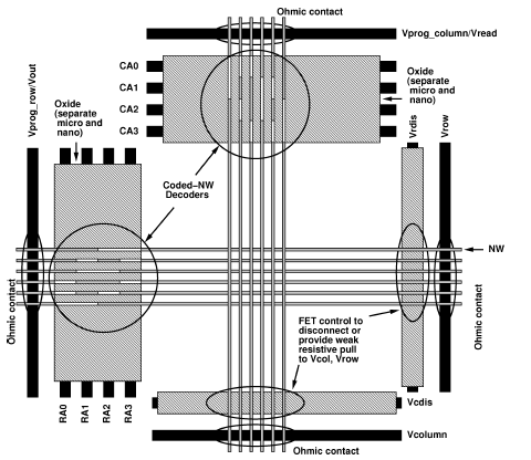
17
|
- PLA with two programmable and restoration/inversion sections
- Address discovery followed by programming
- Two-phase clocking will implement sequential logic
|
|
18
|
- Signal routing possible in X- and Y-direction as well as corner turning.
|
|
19
|
|
|
20
|
- If NWs connected to CMOS wires, lots of time needed for charge
accumulation
- Better solution: use many identically programmed NWs as collective FET
- How does one enter multiple independent inputs?
|
|
21
|
- NW sparing
- Both OR output and restoration NWs must work correctly.
- If Pw is prob NW is not defective, (Pw)2
is prob that OR output is useable
- How many NW pairs needed for correct operation?
- NW failure
- Pc = prob NW makes good contact on one end
- Pj = prob no break in NW of length L0.
- Pctrl = prob NW aligned adequately
- For NW length L = ρ L0, Pw = (Pc)2
x (Pj)ρ x Pctrl
|
|
22
|
- No. non-defective wired-OR NWs
- No. uniquely addressable NWs
- No. non-defective restored NW pairs
- No. uniquely restored terms
|
|
23
|
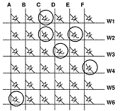
- Goal: reconfigure to route around defects
- E.g. OR-term f = A+B+C+E can be assigned to W3 despite defect
|
|
24
|
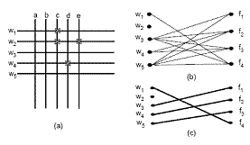
- This is a matching problem.
- Fig (a) shows defects
- Fig (b): NWs to which OR terms can be mapped
- f1 = a+b+c+d, f2 = a+c+e, f3 = b+c, f4
= d+e
- Fig (c): A matching
|
|
25
|
- Our binary model is accurate if each MW provides good control.
- Realistically, some MWs may only partially turn off some NWs.
- Also, some MWs may occasionally fail to control some NWs.
- Our decoders must be fault-tolerant!
|
|
26
|
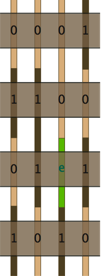
- To apply the ideal model to real-world decoders, consider binary
codewords with random errors.
- If cij = e, the jth MW increases ni‘s
resistance by an unknown amount.
- Consider input A such that the jth MW carries a field. A
functions reliably if a MW for which cik = 1 carries a field.
|
|
27
|
- Consider two error-free codewords, ca and cb. Let
|ca - cb] denote the number of inputs for which caj
= 1 and cbj = 0.
- The balanced Hamming distance (BHD) between ca and cb
is 2•min(|ca - cb], |cb - ca]).
- If ca and cb have a BHD of 2d + 2 they can
collectively tolerate up to d errors.
|
|
28
|
- In a randomized-contact decoder, cij = 1 with some fixed
probability, p.
- If each pair of codeword has a BHD of at least 2d + 2, the decoder can
tolerate d errors per pair.
- This holds with probability > 1- f
when
|

 Notes
Notes